Technology Platform CHyN Clean room
The CHyN clean room is a state-of-the-art ISO Class 4 facility dedicated to complex nanofabrication and interdisciplinary research. Operated jointly by Universität Hamburg (UHH), Deutsches Elektronen-Synchrotron (DESY), and the Max Planck Institute for the Structure and Dynamics of Matter (MPSD).
The lab is located in the Center for Hybrid Nanostructures (CHyN), Building 600, on the research campus Science City Hamburg Bahrenfeld (SCHB).
Management and Coordination
The CHyN clean room is operated by a team of engineers and senior researchers from Universität Hamburg, Deutsches Elektronen-Synchrotron, and the Max Planck Institute for the Structure and Dynamics of Matter, under the supervision of the clean room board, which defines the scientific direction and strategic development of the facility.
The clean room coordinator acts as the central point of contact between users, staff, facility management, and the board, and is responsible for daily operations and ensuring efficient facility use.
Content
List of Equipment
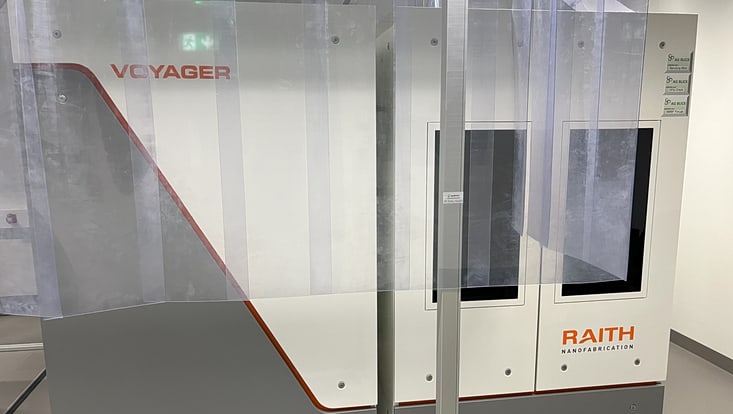
Photo: UHH/Akinsinde
Raith Voyager Electron Beam Lithography System
Field of Application: High-precision 50 kV electron beam lithography system with a nominal accuracy of 2 nm and minimum feature size of 6 nm (≈10 nm achieved internally). Supports substrate sizes from 5 mm to 4 inches. Automatic Height Sensing (2024 upgrade) enables optimized focus across the wafer and reduces stitching errors. TRAXX (FBMS) allows seamless patterning of centimeter-scale paths, and PERIODIXX (MBMS) enables stitch-free periodic structures over large areas
Location: EBL Voyager lab, CHyN Bldg. 600, RM EG. 063

Photo: UHH/Stützle
Raith Picomaster Nanopattern Generator:
Field of Application: High-precision maskless laser lithography system for research and prototyping, supporting substrates up to 125 × 125 mm². Resolution up to 2 nm with scan speeds 20–200 mm/s and flexible step sizes
Location: CHyN Clean room, Yellow room, CHyN Bldg. 600, RM EG. 034

Photo: UHH/Stützle
UV Lithography Mask Aligner MJB4 from Karl Süss company
Field of Application: UV lithography system (UVA 365 nm, UVB 313 nm) supporting contact/proximity exposure with feature sizes 1–5 µm. Handles wafers up to 100 mm (4") with precise XYZ alignment for microfluidics, MEMS, microfabrication and many more applications.
Location: CHyN Clean room, Yellow room, CHyN Bldg. 600, RM EG. 034
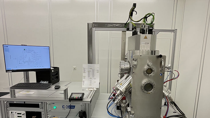
Photo: UHH/Stützle
High-vacuum Coating System from Creavac: Creamet 450 E-Beam S3 Coating System
Field of Apllication:The CREAMET 450 e-beam S3 from CREAVAC is a high-vacuum coating system for precise thin-film deposition on substrates up to 4 inches. It combines a 6-pocket electron beam evaporator, three magnetron sputter sources (RF, DC, HiPIMS), and an ion beam source, allowing uniform deposition of metals and functional materials. The CREACONTROL system ensures precise process control, real-time monitoring, and reproducible coatings.
Location: CHyN Clean room, White room, CHyN Bldg. 600, RM EG. 035

Photo: UHH/Stützle
AT200M Atomic Layer Deposition (ALD) System
Field of Application: AT200M – Compact tabletop ALD system for single 2” wafers, supporting Pt, Hf, Ti, Si (Al in future) with H₂O, O₂, and O₃ reactants.
High-vacuum, heated chamber and manifolds enable precise thin-film deposition, e.g., 10 nm Ti in ~20 min.
Location: CHyN Clean room, White room, CHyN Bldg. 600, RM EG. 035

Photo: UHH/Stützle
Plasma Enhanced CVD Systems SI 500D 214 from Sentech
Field of Application: The inductively coupled plasma enhanced CVD (PECVD) system SI 500D 214 from Sentech is a low-damage, low-temperature PECVD system for depositing dielectric and passivation layers (SiOx, SixNy, SiC, doped layers).
- PTSA plasma source provides homogeneous high-density plasma with low ion energy.
Temperature-controlled substrate with He backside cooling ensures high-quality deposition. - Automated vacuum system supports NH₃, SiH₄, CF₄, O₂, and Ar process gases
Location: CHyN Clean room, White room, CHyN Bldg. 600, RM EG. 035
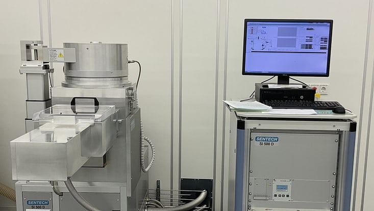
Photo: UHH/Stützle
Reactive Ion Etcher SI 500 215
Field of Applications: The Sentech SI 500D 214 enables low-temperature, low-damage deposition of dielectric and passivation layers such as SiOx, SixNy, SiC, and doped films.
The system key features include:
- Its PTSA plasma source provides uniform, high-density plasma with low ion energy, ensuring high-quality, low-stress layers.
- The dynamic, temperature-controlled substrate with helium backside cooling allows precise layer growth.
- Fully automated vacuum system and versatile process gases (NH₃, SiH₄, CF₄, O₂, Ar) ensure reproducible and efficient deposition.
Location: CHyN Clean room, Yellow room, CHyN Bldg. 600, RM EG. 035

Photo: UHH/Akinsinde
FIB-SEM - ZEISS Crossbeam 550 coupled FIB
Field of Application: Zeiss Crossbeam 550 – High-resolution FIB-SEM (<10 nm) for imaging conductive and non-conductive materials, with optional ion beam milling. The Integrated EDS system enables elemental analysis of thin films, microstructures, and nanostructures..
Location: EBL Voyager lab, CHyN Bldg. 600, RM EG. 060